
Article
Beyond Traditional SEM
What the Apreo S2 Trinity detection system adds for battery materials, polymers, and failure analysis
Blaise Mibeck · Cubic Labs LLC · November 2025
Download PDF All articles and white papers
Through my work at Cubic Labs LLC and the Purdue Electron Microscopy Center (PEMC), I am learning to operate a new SEM, the Thermo Fisher Apreo S2 with its Trinity detection system. The additional imaging modes are a serious advance in electron microscopy, and they are worth knowing about if you send materials out for SEM.
Traditional SEM detection
Most SEM work uses two imaging modes: backscattered electron (BSE) imaging for compositional contrast, and secondary electron (SE) imaging, usually with an Everhart-Thornley detector (ETD), for topographic detail. Interpreting the images requires understanding the physics behind each mode. Both modes also have limits that matter for complex materials such as battery components, where composition, morphology, and surface charge all matter at once.
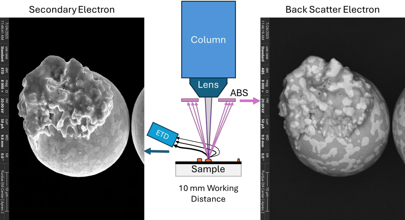
When the primary beam strikes the sample, it produces backscattered electrons with a range of energies and angles, plus secondary electrons at lower energies (Figure 1). Most SEMs collect them in two ways.
The ETD sits to the side of the chamber and collects low-energy secondary electrons attracted by a positive bias. It gives excellent topographic information: surface features, texture, and three-dimensional morphology. Secondary electrons come from inelastic collisions between the beam and electrons near the surface. Most of the beam energy is lost as heat, and the slow secondary electrons resemble a puff of dust kicked up from the surface. The biased ETD vacuums up this dust. Because the ETD is side-mounted, it collects from a limited angular range, and its sensitivity to working distance and sample geometry can produce shadowing.
Traditional below-the-lens BSE detectors collect high-energy electrons that bounced back from the sample. Backscattered electrons are primary-beam electrons scattered elastically by atomic nuclei, and heavier nuclei scatter more strongly, so heavier elements look brighter. This gives compositional contrast. Because the detector looks straight down at the sample, BSE images look flat. These detectors sit below the final lens, far from the sample, so they collect only a fraction of the signal. The signal-to-noise ratio is lower, which is a problem at the low beam voltages that beam-sensitive materials need.
Each mode shows some of the other’s contrast. BSE images contain some topographic contrast, and SE images contain some composition contrast. A flat, polished sample maximizes compositional contrast in BSE, and a gold or platinum coating increases topographic contrast in SE.
The Apreo S2 ETD can run with different grid voltages to filter secondary electrons by energy or to repel them entirely. With the electrons repelled, the ETD detects light emitted from the sample, which gives a partial cathodoluminescence capability without color information. The instrument also has two BSE detectors. The Angular Back Scatter (ABS) detector has several sectors that create the illusion of shadows when a more topographic image is needed. The Concentric Back Scatter (CBS) detector has sectors in concentric rings that separate electrons by emission angle.
Both configurations compromise resolution. The ETD needs working distances of 10 mm or more for good signal collection. BSE detection can suffer from poor collection efficiency, which forces higher beam currents or longer dwell times that can damage delicate samples. The Trinity system takes a different approach.
The Apreo S2 Trinity detection system
Trinity places three detectors inside the electron column: two in the lens (T1 and T2) and one in the column (T3). Any BSE detector must be moved out of the way before these detectors operate. An 8 kV bias on the column’s A-tube, which connects T1, T2, and T3, attracts low-energy electrons upward (Figure 2). The design works best at short working distances and offers three advantages.
- Signal collection. T1 sits millimeters above the pole piece and collects higher-energy, high-angle electrons over a much larger solid angle than a below-lens detector. The signal-to-noise ratio stays high at very low beam voltages and currents, which suits delicate samples such as biological tissue, pharmaceuticals, organic compounds, polymers, and battery materials.
- Spatial resolution. T2 is more sensitive to low- and mid-energy secondary electrons. With working distances down to 2 mm and low voltage and current, the Apreo S2 can resolve features down to 2 nm after careful adjustment.
- Charge contrast. T3 responds to the lowest-energy secondary electrons, which reflect differences in retained charge on the sample. Traditional SE detectors such as the ETD usually lose this information. Higher local charge can indicate crystal defects, discontinuous coatings, differences in electrical conductivity, or electric fields in the sample.
All three detectors operate at the same time, so one scan gives three views of the same location, perfectly registered. That saves time during an imaging session. The ETD and BSE detectors still have a place, because their longer working distances give the depth of field that SEM is known for. The Trinity detectors need a sample with a limited range of feature heights. They also work with the energy-dispersive x-ray spectrometer in place.
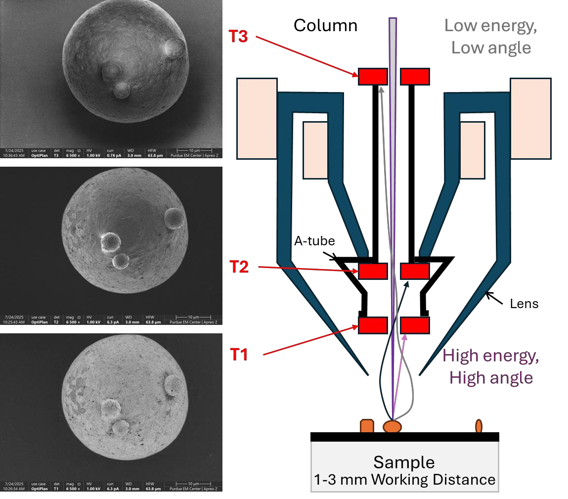
Figure 3 shows LiFePO4 battery cathode particles imaged simultaneously with T1, T2, and T3 at 65,000× magnification and 3 mm working distance. The three images come from the same location at the same moment, yet each looks different because each detector responds to a different electron population.
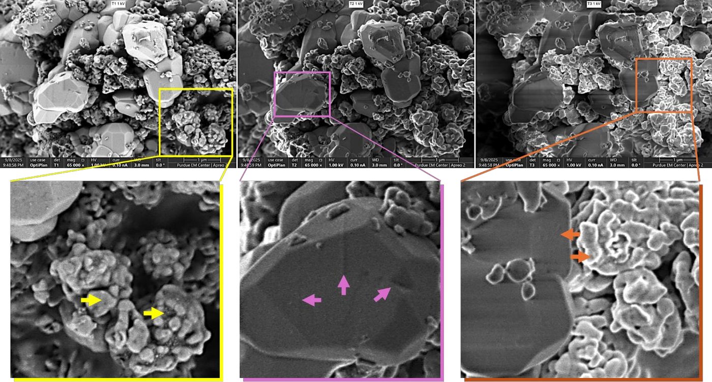
- T1 (left) shows compositional differences between phases. The yellow arrows mark the brighter, iron-rich phase cemented with a darker carbon phase.
- T2 (middle) shows surface topography and particle morphology. The pink arrows mark subtle defects in the larger LiFePO4 crystals and their crisp morphology, which helps identify the equilibrium and growth shapes that matter for understanding how this material forms.
- T3 (right) shows surface charging and ultra-fine surface features. The orange arrows mark the charge difference between the larger, more uniform, conductive crystals and the smaller, less conductive particles.
Impact on materials characterization
I have only begun to explore what the Apreo S2 can do. Some examples of where multi-detector SEM can help:
- For battery research, one acquisition can show the distribution of active material (T1), particle sintering and connectivity (T2), and coating quality (T3), with no extra sample preparation or scans.
- For failure analysis, the three signals separate contamination (compositional), physical damage (topographic), and charging from insulating buildup (T3).
- For polymers, compositional contrast is available at voltages that will not damage the sample. A white paper example showed clear differentiation of an HDPE/COC blend at 500 V.
- For geological, cement, and concrete samples, one acquisition can show mineral phases (T1), grain boundaries and texture (T2), and surface weathering or alteration (T3).
- For quality control, the images give a rapid, non-destructive check of coating uniformity, contamination, and structural defects with little sample preparation.
The SEM images in this article were collected on the Thermo Fisher Apreo S2 FEG-SEM at the Purdue Electron Microscopy Center (RRID:SCR_022687).